


Exploring Electron Dynamics in Graphene
Introduction to Electron Dynamics Measurement
This article presents a comprehensive overview of the advanced experimental setup designed to investigate electron dynamics in graphene. By employing cutting-edge techniques, researchers are able to probe how electrons respond to intense electromagnetic fields, providing invaluable insights into the realm of condensed matter physics.
Experimental Setup
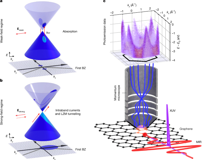
The experimental procedure employs a subcycle momentum microscopy arrangement that utilizes two Yb:KGW amplifiers, producing near-infrared light pulses characterized by a 250 femtosecond duration and a central wavelength of 1,030 nm. Each pulse carries an energy of 1.5 mJ at a frequency of 50 kHz. For the probing phase, a four-stage noncollinear optical-parametric amplifier (NOPA) generates carrier-envelope phase (CEP)-stabilized pulses at 400 nm with a duration of 20 fs.
These pulses are focused into a high-pressure argon jet, yielding high-order harmonics in a vacuum beamline. The seventh harmonic, reaching a photon energy of 21.7 eV, is spectrally filtered to maintain a bandwidth of 0.9 nm. This precise selection allows for pulse durations below 10 fs, after surpassing a thin aluminum foil barrier upon entering the ultrahigh-vacuum (UHV) chamber.
Significance of High Repetition Rates
The momentum microscope has a tendency to record a scant number of electrons per laser shot, necessitating high repetition rates to maintain manageable measurement timelines while ensuring statistical accuracy. This experiment innovatively pushes the boundaries of generating strong, phase-stable mid-infrared (MIR) pump pulses, achieving record average outputs of 1 W with peak electric fields exceeding 200 MV/cm. The result is obtained through difference frequency generation within a gallium selenide crystal.
The pulse duration reaches sub-50 fs, allowing tuning between wavelengths of 4 µm and 15 µm, hence optimizing measurement quality.
Sample Preparation Protocols
Graphene samples are prepared on an n-doped 6H-SiC(0001) substrate, utilizing a method that inhibits conventional rotational alignment. The substrate undergoes a multi-step degassing and annealing process to ensure atomic cleanliness and proper crystallinity before the introduction of borazine to foster the formation of a monolayer graphene aligned to 0° with respect to the substrate lattice.
Post-synthesis, the surface morphology is verified through low-energy electron microscopy, confirming full coverage with the desired monolayer graphene structure.
Electric Field Waveform Reconstruction
The experimental setup effectively allows for in situ reconstruction of electric field waveforms based on the physics of photoemission. As electrons are accelerated in vacuum, their momentum changes in accordance with the applied electric field. This relationship enables the derivation of the electric field waveform through precise calculations.
The reconstructed field can then be employed to correct for momentum streaking within the photoemission spectra, allowing for accurate representation of the material’s electronic band structure.
Interactions and Dynamics in Graphene
To characterize electron-photon interactions, the Keldysh parameter is calculated, distinguishing between weak-field and strong-field regimes in light-matter interactions. The evaluation indicates that the experiment operates well within the strong-field domain, reflecting the significant carrier dynamics that occur during interactions with the MIR field.
Current densities derived from photoemission measurements reveal maximum values significantly exceeding those observed in other materials, validating the high-frequency dynamics intrinsic to graphene.
Conclusions and Future Implications
The innovative methodologies and detailed analyses outlined in this article contribute significantly to the understanding of electron dynamics in graphene. By utilizing advanced experimental setups and rigorous computational models, researchers can unlock new avenues for exploring quantum behaviors in materials. These findings have implications for the development of future optoelectronic devices and quantum technologies.
